Cmos Circuit Schematic Diagram
Cmos crystal frequency multiplier schematic circuit diagram Photos et illustrations 555.fr Cmos circuit transistors sizing size gate questions begingroup
CMOS circuit for Example 2
Cmos capacitance currents coupling Cmos transistor representation Cmos adder technique cdu circuits implementation vlsi
555 timer internal cmos
Verification of this cmos realisationSchematic diagram of existing half adder using static cmos technique Schematic of a cmos inverter circuit showing the main currents andCmos xor gate circuit diagram.
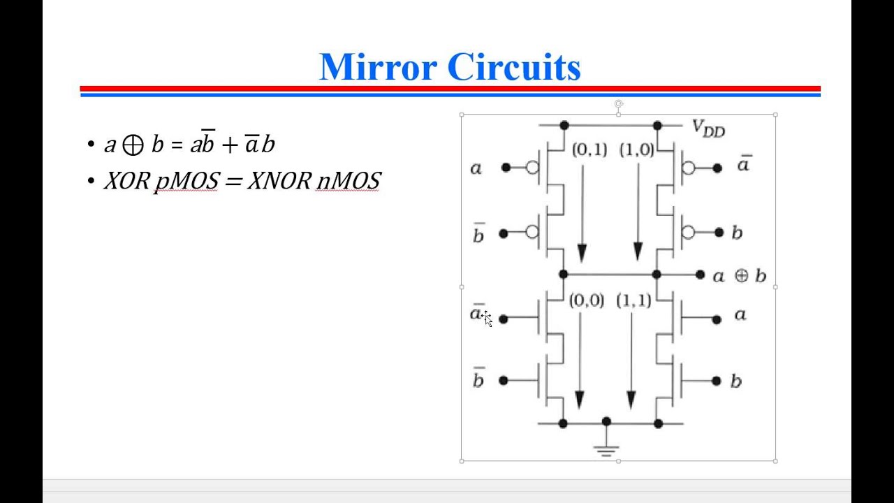
The conventional cmos xor circuit [12].Cmos circuit analysis Cmos xor circuit differentialXor cmos conventional domino exor inputs.

Cmos logic circuits
Cmos layout circuit logicCmos circuit for example 2 Schematic diagram of existing half adder using static cmos techniqueSchematic of a cmos inverter circuit.
Cmos inverter circuit diagram draw explain characteristics transfer its description ques10Cmos circuit question stack Cmos conventional vlsi optimizationXor gate cmos xnor gate exclusive or, png, 800x563px, xor gate, and.

Adder cmos using schematic existing
Cmos inverterFrequency cmos circuit crystal schematic multiplier diagram Cmos logic circuitsSizing transistors for a cmos circuit?.
Xor cmos xnorSolved 1. the basic layout of a cmos circuit is shown below. Draw a circuit diagram of a cmos inverter. draw its transfer(pdf) circuit optimization and design automation techniques for low.

Layout of a cmos logic circuit
Cmos circuit questionCmos realisation verification adresi ota indirme circuitlab created .
.


![The conventional CMOS XOR circuit [12]. | Download Scientific Diagram](https://i2.wp.com/www.researchgate.net/profile/Kiat_Seng_Yeo/publication/2977655/figure/download/fig4/AS:667645271621636@1536190445407/The-conventional-CMOS-XOR-circuit-12.png)